
MeitY Chips to Startup Scheme: How to Join India's Semiconductor Boom
The Ministry of Electronics and Information Technology (MeitY) is steering India towards silicon self-reliance through its Chips to Startup (C2S) Programme. Here is a comprehensive guide for tech founders, researchers, and engineers looking to leverage government EDA tools, financial grants, and fabrication support.
Reading this article: 0s
News in 60 words
~150-word AI digest in one read
Thesis, bullets, quote & takeaway — slogan stays "60 words"
1h ·5 min read· 0 · 0 · 0
Full story
India is currently witnessing an unprecedented push towards self-reliance in deep tech, driven by the government's ₹76,000 crore India Semiconductor Mission (ISM). While giant assembly and fabrication facilities in Gujarat and Assam grab mainstream headlines, the real core of intellectual property creation is happening in design labs across the country. Central to this talent and IP transformation is the Ministry of Electronics and Information Technology's (MeitY) Chips to Startup (C2S) Programme.
Designed to incubate semiconductor design startups and train 85,000 specialized engineers over five years, C2S bridges the gap between academic research, engineering talent, and commercial hardware ventures. For deep-tech entrepreneurs and VLSI engineers in tech hubs like Bengaluru, Hyderabad, and Pune, understanding how to tap into this ecosystem can significantly lower the barrier to entry for building silicon-level products.
What is the Chips to Startup (C2S) Programme?
The C2S Programme is a flagship initiative managed by C-DAC (Centre for Development of Advanced Computing) on behalf of MeitY. Its primary objective is to transform India from a consumer of semiconductor intellectual property (IP) into a global designer and producer of custom chips, Application-Specific Integrated Circuits (ASICs), and System-on-Chips (SoCs).
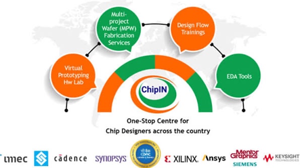
Traditionally, starting a fabless chip company required astronomical capital outlays. Access to Electronic Design Automation (EDA) tools from major vendors like Synopsys, Cadence, or Siemens can cost hundreds of thousands of dollars annually, while multi-project wafer (MPW) runs for fabrication easily run into tens of lakhs of rupees. C2S eliminates these initial financial hurdles by providing subsidized or free access to design tools, cloud infrastructure, and fabrication support.
Core Pillars and Categories of Support
The C2S initiative does not follow a one-size-fits-all model. It categorizes proposals based on technical complexity and institutional readiness across three distinct tracks:
- Category I: SoC/ASIC Development (Advanced Level): Geared towards institutions and deep-tech incubators capable of designing full SoCs, Systems, or complex IPs that target tape-out (fabrication) at semiconductor foundries.
- Category II: Application-Specific IP/ASIC Development (Intermediate Level): Focuses on creating modular IP cores or working prototypes for specific applications like IoT, automotive electronics, smart energy meters, or medical devices.
- Category III: Proof of Concept (PoC) Development (Entry Level): Designed for academic departments and early-stage innovators building field-programmable gate array (FPGA) based prototypes and proof-of-concept hardware designs.
Accessing Government EDA Tools and Infrastructure
One of the most immediate benefits for startups working in partnership with C2S-partnered institutions is the India EDA Grid. Under the programme, centralized cloud infrastructure hosted by C-DAC allows registered research labs and incubated startups to access high-end, industry-standard EDA software suites.
Instead of paying high software license fees, startup teams can log into secure server environments to complete design entry, simulation, synthesis, physical design, and verification. Furthermore, C-DAC provides access to standard cell libraries, IO libraries, and memory compilers required for modern semiconductor layout.
Bridging C2S with the Design Linked Incentive (DLI) Scheme
While C2S focuses heavily on human resource development, academic research, and early prototyping, founders looking to commercialize their designs can seamlessly transition into MeitY's Design Linked Incentive (DLI) Scheme. The DLI scheme offers direct financial support to registered Indian startups:
- Product Design Incentive: Financial support of up to 50% of eligible expenditure, capped at ₹15 crore per application, for chip design and tape-out.
- Deployment Linked Incentive: Financial incentive of 6% to 4% of net sales turnover over 5 years, capped at ₹30 crore per application, for deploying domestically designed chips in commercial products.
Combining C2S infrastructure for initial R&D with DLI funds for final tape-out and deployment drastically reduces dilution risk for early-stage hardware founders seeking seed capital in India.
How Startups and Engineers Can Get Involved
If you are an engineer, researcher, or deep-tech founder looking to leverage the C2S infrastructure, follow these actionable steps:
- Partner with Incubators: Startups can incubate at premier C2S participating institutions such as IIT Madras, IIT Bombay, IISc Bengaluru, or C-DAC facilities to gain access to shared EDA tool clusters.
- Submit Joint Proposals: Apply during periodic C2S call-for-proposals via the dedicated MeitY C2S portal. Proposals must outline clear milestone-based targets, product architecture, and commercialization strategies.
- Target Niche Hardware Requirements: Focus on high-demand domestic sectors such as EV power electronics, NavIC-enabled GPS receivers, smart meter SoCs, and edge AI accelerators where government procurement mandates favor locally designed silicon.
Frequently Asked Questions
Who is eligible to apply for the C2S Programme?
Academic institutions, R&D organizations, and deep-tech startups incubated within recognized academic institutions or government accelerators in India are eligible to apply.
Does the C2S scheme cover chip fabrication costs?
Yes, select proposals under Category I and Category II receive support for tape-out and Multi-Project Wafer (MPW) runs through domestic facilities like SCL Mohali or international foundry partners.
Can foreign-owned companies apply for C2S incentives?
No, the incentives and direct tool access under C2S and the associated DLI schemes are strictly reserved for Indian-owned and controlled entities (where over 50% ownership is held by Indian citizens).
Conclusion
India's journey to becoming a global semiconductor power relies heavily on domestic chip design talent. MeitY's Chips to Startup (C2S) scheme provides the vital structural, financial, and technological backing needed to convert theoretical hardware engineering into commercial silicon. By taking advantage of shared EDA grids, subsidized tape-out support, and downstream DLI incentives, Indian deep-tech entrepreneurs can build world-class hardware products directly out of India.
Support creators
If you found this guide helpful, consider tipping the author on ContentVerse India to support independent technology journalism.
Was this helpful?
Your feedback helps us improve content for everyone.
Liked this piece?
Tip Dhananjay for the work
100% goes to the creator. Send a one-time tip in rupees and back the writing you love.
Dhananjay Singh
0 followers · 0 blogs
Creator on ContentVerse. Building, writing, and shipping in public.
0 followers


Discussion